
Selecting nickel alloys for semiconductor etching equipment is not a simple “best alloy” decision. The right material depends on the etching process, plasma chemistry, component location, temperature, surface finish, contamination limits, mechanical load, cleaning method, documentation requirement and supplier verification.
For buyers, the better question is not:
“Which nickel alloy is best for semiconductor etching?”
A better question is:
“Which material is suitable for this specific component, in this specific plasma or chemical environment, under this exact temperature, contamination and inspection requirement?”
Quick Answer:
There is no single best nickel alloy for all semiconductor etching equipment. Nickel alloys may be evaluated for selected structural, thermal, vacuum, gas-flow, support, fastener, shielding, machined or non-wafer-contact components, but direct plasma-facing applications require process-specific validation. Buyers should review plasma chemistry, fluorine / chlorine / oxygen exposure, temperature, component geometry, surface finish, particle risk, metal contamination limits, cleaning chemistry, MTR / MTC, heat number traceability, PMI, testing and supplier capability before confirming material selection.
ASU Nanofab explains that common dry etch chemistries include fluorine, chlorine, methane / hydrogen and oxygen, and that etch process development must consider chemistry and the material being etched: ASU Dry Etch Techniques.
A 2024 review in Journal of Vacuum Science & Technology B notes that particles and foreign elements introduced by processing equipment can cause random yield loss, and that corrosive processing plasma consumes chamber parts such as walls, chucks and focus rings over time: Future of Plasma Etching for Microelectronics.
This is why nickel alloy selection for semiconductor etching equipment should be based on real process exposure, not only general material datasheets.
Why Material Data Sheets Alone Are Not Enough
Material data sheets are useful. They provide basic chemical composition, mechanical properties, heat treatment condition and sometimes general corrosion information.
However, semiconductor etching equipment is exposed to highly specific process conditions that may not appear on a standard datasheet.
These may include:
- Fluorine-based plasma
- Chlorine-based plasma
- Oxygen plasma
- Mixed-gas plasma
- Ion bombardment
- Sputtering
- Etch byproducts
- Chamber cleaning chemistry
- High local temperature
- Thermal cycling
- Vacuum conditions
- Particle contamination limits
- Metallic contamination limits
- Special surface finish requirements
- Tight dimensional tolerance
- Complex machined geometry
A datasheet can support initial screening, but it should not be treated as final proof of plasma compatibility.
Datasheet Data vs. Real Etching Conditions
| Datasheet Item | Why It Helps | What It May Not Cover |
|---|---|---|
| Chemical Composition | Confirms alloy identity | Trace elements critical to contamination control |
| Tensile Strength | Shows mechanical capability | Plasma erosion or particle behavior |
| Yield Strength | Supports design stress review | Thermal cycling in real equipment |
| Hardness | Helps verify heat treatment condition | Surface reaction under plasma |
| General Corrosion Data | Useful for wet chemical screening | Fluorine, chlorine or oxygen plasma compatibility |
| Density / Thermal Data | Helps design review | Local hot spots in complex geometry |
| Standard Grade | Confirms purchase basis | Whether the exact component is qualified for the tool |
For semiconductor etching equipment, buyers should ask for application-relevant evidence when possible, such as plasma exposure data, chamber history, OEM qualification information, particle performance, surface finish records, cleaning compatibility or third-party testing.
What Makes Semiconductor Etching Environments Different?
Plasma etching is not the same as ordinary liquid chemical exposure.
In plasma etching, gas chemistry, radicals, ions, RF power, chamber pressure, surface reactions and byproducts can all influence how a component behaves.
The Semiconductor Industry Association explains that plasma dry etching and chamber cleaning use fluorinated chemistries, and that these chemistries help enable semiconductor manufacturing process stability and performance: SIA Plasma Etch and Deposition White Paper.
Key Exposure Factors
| Factor | Why It Matters for Nickel Alloy Selection |
|---|---|
| Fluorine Plasma | May attack or modify exposed surfaces depending on alloy and condition |
| Chlorine Plasma | Requires plasma-specific compatibility review, not only liquid chloride data |
| Oxygen Plasma | May promote oxidation or surface modification |
| Ion Bombardment | Can contribute to physical sputtering or erosion |
| Temperature | Affects strength, oxidation, diffusion and thermal stress |
| Thermal Cycling | May create fatigue or dimensional stability concerns |
| Etch Byproducts | May deposit on chamber walls or components |
| Chamber Cleaning | Cleaning chemistry may be different from normal etching chemistry |
| Vacuum Environment | Outgassing and cleanliness may matter |
| Surface Finish | Can influence particle generation, cleaning and residue retention |
| Component Geometry | Sharp edges, thin sections and corners may create local hot spots or stress concentration |
For this reason, a nickel alloy that is acceptable for one component may not be suitable for another component in the same tool.
Are Nickel Alloys Always Suitable for Plasma-Facing Parts?
No. Nickel alloys are not automatically suitable for every plasma-facing component.
Some direct plasma-facing parts may require ceramic materials, coatings or specialized surface treatments depending on the tool design and process chemistry. Nickel alloys may still be useful for selected structural, thermal, vacuum, fastener, support, gas-flow or machined components, but suitability must be confirmed by the process requirement.
Buyers should avoid assuming that general nickel alloy corrosion resistance equals plasma resistance.
A study on plasma-resistant materials notes that materials used in plasma etching equipment are evaluated because erosion and particle generation under fluorine-based plasma can be significant issues: Comparison of Erosion Behavior and Particle Contamination in Plasma-Resistant Materials.
Another study on fluorine plasma etching behavior discusses plasma-resistant materials used in semiconductor plasma etching equipment: Structural and Fluorine Plasma Etching Behavior of Sputter-Deposited Y2O3 Films.
These sources support a practical point: plasma-facing material selection should be validated for erosion, particles and contamination, not only for mechanical strength.
How Do Different Etching Processes Influence Material Choice?
Different etching processes create different risks.
A material that works in a lower-temperature support component may not work in a fluorine-rich plasma area. A component exposed to chlorine plasma may need different validation from one exposed mainly to oxygen plasma.
Process-Driven Material Review
| Etching Process / Exposure | Main Material Questions |
|---|---|
| Fluorine-Based Plasma | Is erosion rate acceptable? Are particles generated? Are metallic contaminants controlled? |
| Chlorine-Based Plasma | Is chlorine plasma compatibility verified? Is high-temperature corrosion risk reviewed? |
| Oxygen Plasma | Is oxidation or surface modification acceptable? |
| DRIE / SF6-Based Etching | Is the component exposed to fluorine species, thermal cycling or chamber cleaning? |
| Mixed-Gas Plasma | Are byproducts, deposits and cleaning cycles considered? |
| Chamber Cleaning | Is the cleaning chemistry more aggressive than normal process exposure? |
| Non-Plasma Structural Area | Are strength, thermal expansion, machining tolerance and vacuum cleanliness more important? |
DRIE and SF6-Based Processes
Deep Reactive Ion Etching, or DRIE, is commonly used for high-aspect-ratio silicon etching. Some DRIE processes use SF6-based etching chemistry, and Bosch-type processes often involve alternating etch and passivation steps.
University and research sources describe Bosch DRIE as a high-aspect-ratio silicon etching method using SF6-based etching and passivation cycles: Berkeley Bosch DRIE Silicon Processing.
For buyers, this means parts exposed to DRIE environments should be reviewed for:
- Fluorine plasma exposure
- Thermal cycling
- Chamber cleaning exposure
- Particle generation
- Surface finish
- Component location
- Maintenance interval
- Tool qualification requirement
Chlorine Plasma
Chlorine-based plasma is used in selected metal or compound semiconductor etching processes. But liquid chloride corrosion resistance does not automatically prove chlorine plasma resistance.
Buyers should ask:
- Is the component directly exposed to chlorine plasma?
- Is there historical performance data in this tool or similar tools?
- Is the component plasma-facing or shielded?
- What cleaning process follows the etch process?
- What particle and contamination limits apply?
- Is a coating or ceramic alternative required?
Oxygen Plasma
Oxygen plasma may be used for ashing, organic removal or other surface processes. It may affect oxidation, surface roughness or polymer-related residues depending on the process and material.
For nickel alloys, buyers should review:
- Oxidation behavior
- Surface finish change
- Particle generation
- Temperature
- Cleaning cycle
- Whether the part is wafer-facing or non-wafer-facing
What Nickel Alloys May Be Evaluated?
Nickel alloys may be evaluated for selected semiconductor equipment components where corrosion resistance, high-temperature strength, mechanical stability, machining quality or vacuum compatibility is required.
However, final selection should follow tool design, OEM requirements, process exposure and qualification testing.
Nickel Alloy Options to Review
| Alloy | Possible Reason to Evaluate | Buyer Caution |
|---|---|---|
| Alloy 625 / UNS N06625 | Corrosion resistance, strength, weldability, machined components, selected support or gas-flow parts | Confirm plasma exposure, surface finish, metallic contamination and ASTM standard |
| Alloy 718 / UNS N07718 | High strength, aging response, fasteners, springs, shafts, high-load or temperature-related parts | Confirm heat treatment, hardness, tensile properties, stress relaxation and cleanliness |
| Alloy 600 / UNS N06600 | High-temperature oxidation and selected corrosion service | Confirm actual plasma chemistry and temperature limits |
| Alloy 601 / UNS N06601 | High-temperature oxidation resistance in selected environments | Confirm compatibility with chamber chemistry and cleaning process |
| Alloy C276 / UNS N10276 | Strong corrosion resistance in selected aggressive chemical environments | More relevant to wet chemical or cleaning exposure than direct plasma unless validated |
| Alloy 825 / UNS N08825 | Selected acid / chloride corrosion environments | Confirm application and contamination limits |
| Nickel 200 / UNS N02200 | Selected high-purity or caustic-related applications | Confirm strength, temperature and contamination requirements |
This table is not a final recommendation. It is a starting point for technical discussion.
Why High-Temperature Strength and Heat Treatment Matter
Some semiconductor equipment parts may experience elevated temperature, thermal cycling or mechanical load.
Nickel-based superalloys are known for high-temperature use. Cambridge University explains that superalloys can be used at high temperatures and that creep and oxidation resistance are important design criteria: Nickel Based Superalloys - University of Cambridge.
ASTM B637 covers precipitation-hardenable nickel alloy rod, bar, forgings and forging stock for moderate or high-temperature service: ASTM B637.
ASTM B446 covers UNS N06625 and related nickel-chromium-molybdenum alloys in rod and bar form, including hot-worked and cold-worked products: ASTM B446.
For buyers, this means the alloy name alone is not enough. They should confirm:
- UNS number
- ASTM / ASME standard
- Product form
- Heat treatment condition
- Aging condition if applicable
- Tensile strength
- Yield strength
- Elongation
- Hardness
- Machining requirement
- Surface finish
- Cleanliness requirement
- Batch traceability
Why Particle and Contamination Risk Must Be Reviewed
Semiconductor etching equipment is highly sensitive to particles and contamination.
The 2024 AIP review notes that particles and foreign elements introduced by processing equipment can cause random yield loss and should be monitored and constrained: Future of Plasma Etching for Microelectronics.
A CS MANTECH paper also notes that particles in plasma etch may originate from chamber walls, lids, gas inlets, electrostatic chucks, plasma or the wafer itself: Reduction in Scattered Particles Contamination in Dry Etch Chambers.
Buyer Questions on Contamination
| Question | Why It Matters |
|---|---|
| Is the component wafer-facing? | Wafer-facing parts have higher contamination sensitivity |
| Is the component plasma-facing? | Plasma exposure may cause erosion or particles |
| Is nickel contamination acceptable in this tool area? | Metallic contamination limits may vary by process |
| Is the surface polished, coated or cleaned? | Surface condition can affect particles and residues |
| Is there a clean packaging requirement? | Packaging can affect cleanliness before installation |
| Are trace elements controlled? | Some trace elements may matter for semiconductor applications |
| Is outgassing a concern? | Vacuum process compatibility may require review |
| Is the part cleaned after machining? | Machining oils and residues must be controlled |
A material may meet ASTM chemistry and mechanical requirements but still be unsuitable if contamination, cleanliness or particle limits are not met.
What Surface Finish Should Buyers Specify?
Surface finish should not be vague.
For semiconductor-related equipment components, buyers may need to specify:
- Machined surface finish
- Polished surface
- Electropolished surface if applicable
- Deburring requirement
- Edge radius
- Ra value
- Cleaning method
- No visible scratches, cracks, burrs or machining residues
- Clean packaging
- End caps or sealed bags
- Lot marking and traceability
Surface finish affects cleaning, particle retention, local heating, plasma exposure behavior and component fit.
Buyers should avoid only writing “good surface.” Instead, they should define measurable surface and cleanliness requirements.
How Can Buyers Verify Supplier Claims?
Supplier claims should be supported by documents and test data.
An ISO 9001 certificate may show that a supplier has a quality management system, but it does not prove that a specific batch of nickel alloy will perform in a semiconductor plasma etching environment.
ISO explains that the ISO 9000 family helps organizations improve product and service quality and meet customer expectations: ISO 9000 Family.
However, buyers still need batch-specific documents.
Documents and Data to Request
| Data / Document | What It Confirms |
|---|---|
| MTR / MTC | Batch-specific chemistry and mechanical properties |
| Heat Number | Traceability to melt or production batch |
| UNS Number | Correct alloy identity |
| ASTM / ASME Standard | Product form and technical basis |
| Heat Treatment Record | Supplied condition |
| Tensile Test | Strength and ductility |
| Hardness Test | Condition and consistency |
| PMI / Grade Verification | Material identity check |
| Dimensional Report | Compliance with drawing |
| Surface Finish Report | Ra, polishing or machining requirement |
| Cleaning Record | Cleanliness requirement if specified |
| NDT Report | UT, PT, RT or other test if required |
| Third-Party Report | Independent verification when required |
| Plasma Exposure Data | Application-specific evidence if available |
| Particle / Contamination Data | Required for sensitive components if available |
ASTM E1476 provides guidance for nondestructive identification and sorting of metals: ASTM E1476.
ASTM E213 covers ultrasonic testing of metal pipe and tubing: ASTM E213.
ASTM E8/E8M covers tension testing of metallic materials, including yield strength, tensile strength, elongation and reduction of area: ASTM E8/E8M.
What Supplier Questions Should Buyers Ask?
Before sourcing nickel alloy materials for semiconductor etching equipment, buyers should ask detailed questions.
Supplier Verification Checklist
| Category | Questions to Ask |
|---|---|
| Material Grade | What is the exact grade and UNS number? |
| Product Form | Bar, forging, tube, pipe, plate or machined part? |
| Standard | Which ASTM / ASME / customer standard applies? |
| Heat Treatment | What condition is supplied? Annealed, solution annealed, aged or stress relieved? |
| Traceability | Can each part be traced to heat number and MTR? |
| Surface Finish | What Ra, polishing, deburring or cleaning is included? |
| Cleanliness | Is clean packaging available? Are residues controlled? |
| Testing | Which chemical, mechanical, PMI, NDT or dimensional tests are included? |
| Plasma Data | Is there any data for fluorine, chlorine or oxygen plasma exposure? |
| Contamination | Can trace elements or impurity levels be controlled? |
| Machining | Can tolerances, burr control and edge treatment be maintained? |
| Third-Party Inspection | Can SGS, BV, TÜV, LRQA, ABS or buyer-appointed inspection be supported? |
| Delivery | What is the production lead time and logistics plan? |
| Change Control | How are material lot, process or subcontractor changes communicated? |
A reliable supplier should not only quote price. They should help clarify process exposure, material standard, testing, documentation and packaging scope.
Common Procurement Pitfalls
1. Treating “Plasma Resistant” as a Generic Claim
“Plasma resistant” is not specific enough.
Buyers should ask:
- Resistant to which plasma?
- Fluorine, chlorine, oxygen or mixed gas?
- At what temperature?
- For which component location?
- Under what RF power, pressure and process time?
- What particle or contamination limit?
- What evidence supports the claim?
2. Using Liquid Corrosion Data Alone
Liquid corrosion resistance data does not fully represent plasma exposure.
It may be useful for wet cleaning, chemical handling or non-plasma areas, but direct plasma-facing applications need plasma-specific evaluation.
3. Ignoring Component Location
A part outside the direct plasma zone may need strength, machining accuracy and cleanliness. A part inside the plasma zone may need erosion resistance, particle control and coating compatibility.
4. Ignoring Surface Finish
Machining marks, burrs, scratches or residues may affect particles, cleaning and local surface reactions.
5. Assuming ISO 9001 Replaces Batch Records
ISO 9001 supports quality management, but buyers still need MTR / MTC, heat number traceability, dimensional reports, surface inspection and test records.
6. Comparing Only Unit Price
A low initial price may become costly if the material causes qualification delays, repeated replacement, chamber contamination or unplanned maintenance.
The U.S. Environmental Protection Agency defines life-cycle cost as original cost minus salvage value plus operating costs, maintenance costs, renewal costs and decommissioning costs: EPA Life Cycle and Replacement Costs.
The U.S. Department of Energy’s O&M Best Practices Guide describes reactive maintenance as allowing machinery to run to failure and repairing or replacing damaged equipment when obvious problems occur: DOE O&M Best Practices Guide.
For semiconductor equipment parts, buyers should compare material price with lifetime, qualification cost, maintenance interval, downtime risk, contamination risk and delivery reliability.
RFQ Checklist for Nickel Alloys in Semiconductor Etching Equipment
Before requesting a quotation, buyers should prepare the following information.
| RFQ Item | What to Provide |
|---|---|
| Component Name | Shield, ring, fastener, support, bracket, tube, gas part, machined part |
| Drawing | Full dimensions, tolerance, surface finish and edge requirements |
| Material Grade | Alloy 625, Alloy 718, Alloy 600, Alloy 601, C276 or open to recommendation |
| UNS Number | Exact material designation |
| Product Form | Bar, forging, tube, pipe, plate or machined part |
| Standard | ASTM / ASME / customer specification |
| Component Location | Plasma-facing, wafer-facing, shielded, vacuum area or external support |
| Plasma Chemistry | Fluorine, chlorine, oxygen, SF6, CF4, NF3, Cl2, BCl3, O2 or mixed gas |
| Temperature | Normal, maximum, cleaning and cycling temperature |
| Mechanical Load | Stress, fastening, support, vibration or thermal cycling |
| Surface Finish | Ra, polishing, deburring, electropolishing if required |
| Cleanliness | Cleaning method, packaging, residue control |
| Contamination Limits | Metal impurity or particle requirement if applicable |
| Testing | Chemical, mechanical, hardness, PMI, NDT, dimensional inspection |
| Documentation | MTR / MTC, heat number, inspection report, certificate |
| Third-Party Inspection | Required or optional |
| Delivery | Required date, destination and packaging method |
This checklist helps suppliers quote the same technical scope and reduces misunderstanding.
Example RFQ Wording
For Alloy 625 bar stock:
“Please quote Alloy 625 / UNS N06625 bar according to ASTM B446 for semiconductor equipment machined components. Application: selected support component in etching equipment. Please confirm heat treatment condition, chemical analysis, tensile test, hardness, MTR / MTC, heat number traceability, PMI, dimensional inspection and clean packaging. Surface finish and final machining requirements are shown in the attached drawing. Please quote third-party inspection option.”
For Alloy 718 machined parts:
“Please quote Alloy 718 / UNS N07718 machined parts according to ASTM B637, aged condition as specified in drawing. Application: high-strength component for semiconductor equipment. Please provide MTR / MTC, heat number traceability, heat treatment record, tensile test, hardness test, PMI, dimensional report, surface inspection and clean packaging. Please confirm whether any plasma exposure qualification data is available.”
For plasma-exposed components:
“Please confirm whether the proposed nickel alloy has been validated for the stated plasma chemistry, temperature, component location and contamination limit. If direct plasma exposure is expected, please provide available erosion, particle, surface change or application history data. If data is not available, please quote material supply only and identify that plasma compatibility must be confirmed by customer qualification.”
This is clearer than simply writing:
“Please quote nickel alloy parts for semiconductor etching equipment.”
How Emily PIPE Supports Semiconductor Equipment Material Buyers
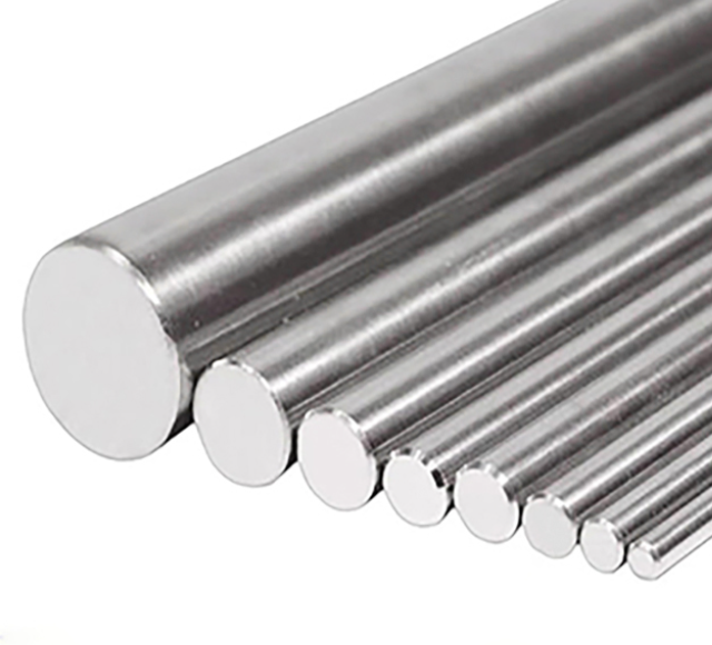
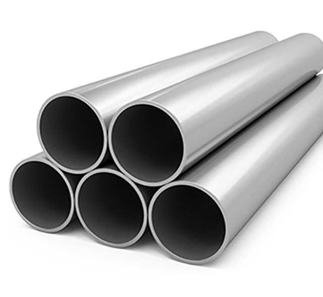
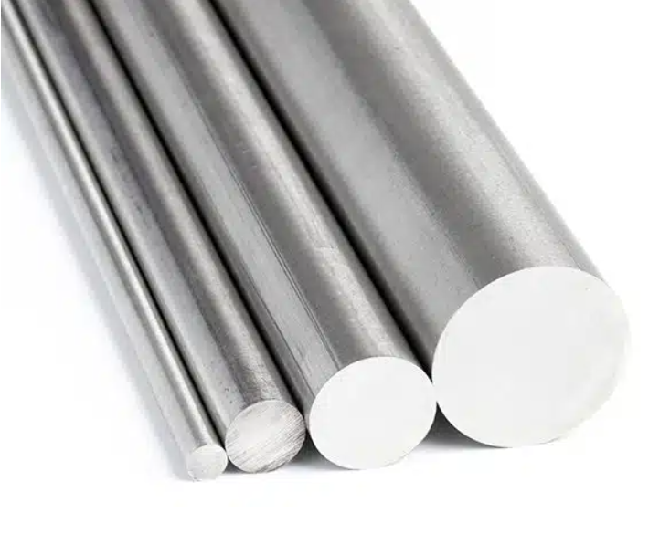
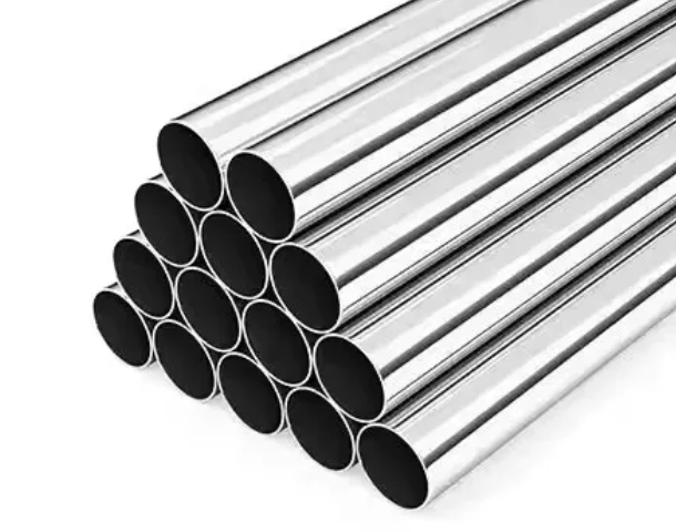
Emily PIPE is a China-based manufacturer and exporter specializing in nickel alloy tubes, nickel alloy bars, titanium alloy tubes and titanium alloy bars. We support customers across chemical processing, oil and gas, marine engineering, aerospace, power generation, medical equipment, heat exchangers, semiconductor-related equipment and other corrosion-resistant or high-temperature applications.
For semiconductor equipment material sourcing, we can support:
- Nickel alloy bars
- Nickel alloy tubes and pipes
- Titanium alloy bars and tubes
- Materials for machined parts
- Materials for support, structural, gas-flow or thermal components
- Alloy 625, Alloy 718, Alloy 600, Alloy 601, Alloy 825, Alloy C276 and other grades according to project requirements
- ASTM / ASME material standard support
- Custom OD, wall thickness, length, tolerance and surface condition
- MTR / MTC and heat number traceability
- Dimensional and surface inspection
- PMI, chemical analysis, tensile, hardness, UT, ECT, hydrostatic and other testing support when required
- Third-party inspection support
- Export packaging and logistics support
Our role is not to claim that one nickel alloy is best for every semiconductor etching application. Our role is to help buyers clarify material grade, standard, component location, plasma or chemical exposure, surface finish, testing, documentation and delivery needs before production.
If you are sourcing nickel alloy or titanium materials for semiconductor equipment, please send the drawing, material grade, UNS number, product form, required standard, component location, plasma chemistry, temperature, surface finish, contamination requirement, testing requirement, documentation requirement and destination. Our team can help review your requirements and provide a suitable quotation.
FAQ: Nickel Alloys for Semiconductor Etching Equipment
1. Is there one best nickel alloy for semiconductor etching equipment?
No. The suitable material depends on plasma chemistry, component location, temperature, surface finish, contamination limit, mechanical load and qualification requirements.
2. Can nickel alloys be used for direct plasma-facing components?
Sometimes they may be evaluated, but direct plasma-facing use requires process-specific validation. Many plasma-facing components may use ceramics, coatings or specialized materials depending on tool design.
3. Is Alloy 625 suitable for semiconductor etching equipment?
Alloy 625 may be evaluated for selected corrosion-resistant or structural components, but buyers must confirm plasma exposure, contamination limit, surface finish, temperature and documentation requirements.
4. Is Alloy 718 suitable for semiconductor equipment parts?
Alloy 718 may be evaluated for high-strength or temperature-related components, but heat treatment condition, hardness, mechanical properties and cleanliness requirements must be confirmed.
5. Are general corrosion datasheets enough?
No. Datasheets are useful for initial screening, but semiconductor etching requires review of plasma chemistry, sputtering, erosion, particles, contamination, temperature and component location.
6. What documents should buyers request?
Buyers should request MTR / MTC, heat number traceability, chemical composition, mechanical properties, heat treatment records, PMI, dimensional report, surface inspection and NDT reports when required.
7. Why does surface finish matter?
Surface finish can affect cleaning, particle retention, local surface reactions and installation fit. Buyers should specify Ra, polishing, deburring, edge treatment and clean packaging when needed.
8. What should be confirmed before placing an order?
Buyers should confirm material grade, UNS number, standard, component drawing, plasma exposure, temperature, surface finish, contamination limits, testing, documentation, inspection and packaging requirements.
Conclusion
Nickel alloy selection for semiconductor etching equipment should not be based only on alloy name or general datasheets.
The right decision depends on plasma chemistry, component location, temperature, mechanical load, surface finish, contamination sensitivity, cleaning chemistry, MTR / MTC, heat number traceability, testing and supplier capability.
For buyers, good sourcing means combining application data, verifiable documentation, batch traceability and careful supplier communication before production.